Page 12 of 23
Re: Toshiba MOSFETs with a twist
Posted: Mon Jul 31, 2017 1:42 pm
by nige2000
not sure im fully with you is it like this

Re: Toshiba MOSFETs with a twist
Posted: Mon Jul 31, 2017 1:55 pm
by abraxalito
No caps in the data lines. The HC86 has 4 gates inside, 3 of them are configured as buffers (CK, WS, D+). The 4th one is arranged to invert (D-).
Re: Toshiba MOSFETs with a twist
Posted: Mon Jul 31, 2017 3:08 pm
by nige2000
So no need for the caps and just connect CK and ws to gate a which is positive?
And data to a on one gate and b on another gate for neg
Sorry for silly questions
Re: Toshiba MOSFETs with a twist
Posted: Mon Jul 31, 2017 3:37 pm
by abraxalito
If you refer to NXP DS for the HC86, each gate is labelled A,B for the inputs and Y for the output.
Gate 1 is arranged to invert so 1A goes to VDD (pin14), 1B goes to 2B and also the 'Data' input. 2A goes to GND (pin7). 1Y is negative data, 2Y is positive data to the 1387s (pin3).
On the other side of the chip, 4B is the WS input, 4A goes to 0V. 4Y goes to the DACs WS input (pin2). 3B is the CK input, 3A goes to 0V and 3Y goes to pin1 of the 1387s (CK).
I have a 2.5V power supply for the HC86 as the 1387s inputs are TTL. Put series resistors in between the data source and the HC86 (say 330R) as current limiters in case the data source voltage '1' level exceeds 2.5V.
Re: Toshiba MOSFETs with a twist
Posted: Mon Jul 31, 2017 6:27 pm
by nige2000
ah ok you determine inverted or noninverted by pulling up or down pin *"A"
Re: Toshiba MOSFETs with a twist
Posted: Tue Aug 01, 2017 1:00 am
by abraxalito
Yep that's the nature of an XOR gate, otherwise known as a 'conditional inverter'. Could just as easily have been B, the inputs are symmetrical.
Re: Toshiba MOSFETs with a twist
Posted: Fri Aug 04, 2017 4:51 am
by abraxalito
V2.0 of the I/V stage is now taking shape.
I designed the previous version in stages and never simulated the filter feeding into the I/V stage. While V1.0 sounded great its max output voltage was almost 3X (10dB) lower than I had designed for - I originally figured I must have made a wiring error. In fact I had - I had fitted the first batch of fake Taobao MOSFETs instead of the real Toshibas. The fakes have higher threshold voltage and lower gm so I figured that putting the designed-for FETs in would fix up the level. But they didn't. After a LOT of head scratching I decided to sim the whole thing, filter and I/V stage combined and sure enough, the sim showed the same lower output level. I have now figured out what was wrong - the gm doesn't tell the whole picture about the input impedance of a common-gate MOSFET, the output resistor can also influence it. Hence V2.0 which sims fine so hopefully will deliver the full 1V output peak level. This no longer uses just two cheap inductors as I've modified the filter to use the output current from the DACs more efficiently. The old filter was throwing half away due to the need for low impedance matched terminations - one good side effect is I no longer need the large 'lytics on the input.
- DACv2.0.jpg (75.16 KiB) Viewed 678 times
Re: Toshiba MOSFETs with a twist
Posted: Fri Aug 04, 2017 10:58 am
by nige2000
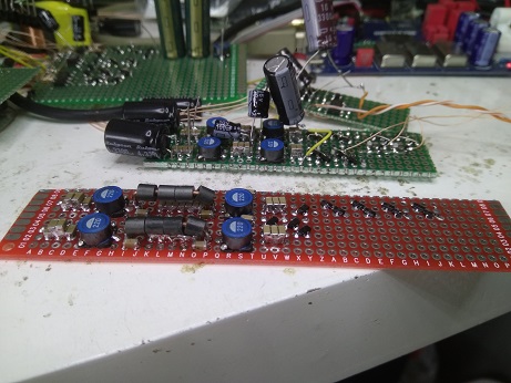
first attempt of gain stage failed :(
sent u across schematic
will start again with adapterboards
Re: Toshiba MOSFETs with a twist
Posted: Fri Aug 04, 2017 1:35 pm
by abraxalito
Got your email. The beauty of transformers is - they just work, like passive filters. So although its a work-up getting wire and winding the time saved at the back-end of the build is immense.
Re: Toshiba MOSFETs with a twist
Posted: Fri Aug 04, 2017 11:50 pm
by nige2000
Id like to get this working
Started attempt 2 with adapter boards
This way I can change out all parts easily
I'm using a variable bench supply initially for testing using positive 24v as GND
Used resistors to bias the input to 4.2v otherwise its an exact replica of your schematic