Toshiba MOSFETs with a twist

Re: Toshiba MOSFETs with a twist
Intriguing - wouldn't mind listen at some stage John
Do or do not, there is no try
Re: Toshiba MOSFETs with a twist
Sure, Fran - I'll send one down with one of the Oompa Loompa's doing the soldering at the weekend.
Which one got the golden ticket?
I believe you'll find the sound of SE Class A intriguing
www.Ciunas.biz
For Digital Audio playback that delivers WHERE the performers are on stage but more importantly WHY they are there.
For Digital Audio playback that delivers WHERE the performers are on stage but more importantly WHY they are there.
-
abraxalito
- Posts: 230
- Joined: Fri Sep 16, 2016 11:05 pm
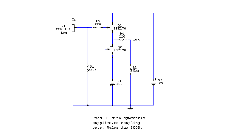
Active I/V stages - why MOSFETs are a reasonable choice
For those who are curious enough there's a very long thread over on DIYA about discrete I/V stages for I-out DACs, mostly the designs are based on JFETs : http://www.diyaudio.com/forums/digital- ... erter.html
Pretty much everyone agrees JFETs as I/V sound awesome though I've not found a convincing explanation for why in my searching. Possibly it has something to do with JFETs not having forward biassed P-N junctions so they're not prone to rectifying RF (DACs are incredibly noisy in the RF spectrum, being part digital).
There are issues with using JFETs that it seems to me that MOSFETs solve. First is availability - MOSFETs are still a growth area and active product development is continuing. For JFETs, not so much, parts are getting discontinued, particularly P-channel devices. With MOSFETs its seeming like the opposite is taking place - P-channels are becoming even more popular than N in the lower voltage ratings which are of interest for I/V applications. Of course being 'unobtainium' holds a certain appeal for some audiophile types.
A second issue is a technical one. JFETs in general exhibit poor gm (transconductance). You might wonder why this matters? In an active I/V the input goes to the source of the FET and the input impedance seen by the DAC is inversely proportional to the gm. DACs love to feed into low impedances (TDA1543 passive I/V designs not withstanding). The 'objectivist' reason for why DACs should see the lowest possible impedance is that this minimizes the effect that the output impedance is varying with digital code. Translated it means lower THD figures. Subjectivists (like myself) don't pay too much attention to THD figures but it turns out that there's another reason lower impedances are better - they mean better PSRR for the DAC. In terms of SQ this translates to better bass and generally improved dynamics.
So when we use a JFET in an I/V stage we want to do our best to give the circuit the lowest possible input impedance and this is generally done by paralleling JFETs. Paralleled FETs means their gms are summed but there are some practical difficulties. Firstly paralleled JFETs have a tendency to oscillate so need careful management. The oscillation frequencies are so high they may easily be missed by DIYers with affordable 'scopes. Secondly JFETs in parallel need matching - this is fun for some DIYers though so adds to the appeal. Not everyone wants to fiddle around with tweezering tiny SMT packages into test sockets though.
If you dig into that DIYA thread you'll see one suggestion is an array of 4 or 8 2SK209 JFETs as I/V. Let's examine the numbers for that idea in the next post and see how a Toshiba MOSFET might size up alongside that solution...
Re: Toshiba MOSFETs with a twist
Great stuff, Richard, looking forward to the next installment.
www.Ciunas.biz
For Digital Audio playback that delivers WHERE the performers are on stage but more importantly WHY they are there.
For Digital Audio playback that delivers WHERE the performers are on stage but more importantly WHY they are there.
-
abraxalito
- Posts: 230
- Joined: Fri Sep 16, 2016 11:05 pm
Toshiba MOSFETs vs JFETs for I/V
Here's the Yfs (gm) plot of a 2SK209
Notice that the Yfs varies with drain current, to get higher Yfs we need higher current. This is true for all transistors whether bipolar or FET. Bipolars though have the highest slope meaning for a given current they'll have the highest gm and there's a simple formula for that : gm = 40*Ic.
JFETs are available in various grades related to their maximum drain current with zero gate bias. In Toshiba's world the -BL suffix has the highest current so is the normal choice for circuits that want high gm. I went over to Mouser and turns out they don't list the -BL, only the two lower grades (-GR and -Y). The -Y is next to useless in this application but the -GR could be used. Over at Digikey they do have the -BL in stock but you'll need to order a reel of 3k parts (just a shade under $500). -GR is available individually at $0.55. So now we know we can only practically obtain the -GR from these guys, this tells us we'll be limited to 6mA or so, that'll give us the effective gm which from the plot, is 20mS.
A 20mS gm corresponds to an input impedance of 50ohms (Zin = 1/gm). This is a bit high for some DACs so the reason for paralleling becomes clear. With 4 in an array we'll reach 12.5ohm assuming matching is decent. We'll also be sipping 24mA through those 4 devices. Note that a single bipolar transistor running at 24mA will have gm = 0.96S and give a Zin = 1ohm. So the JFETs are about 12X worse at achieving low Zin for the same current.
The other issue of interest to designers of I/V stage is parasitic capacitance. Paralleling devices multiplies up the capacitance, which for a single 2SK209 is around 4pF for the feedback capacitance (Crss). Input capacitance isn't too material because in an I/V stage there's no appreciable voltage change across it, its effectively bootstrapped by the gm. The figure of merit for an I/V transistor is how much gm per pF of feedback capacitance - 2SK209 has (20mS/4pF) = 5 kudos points. Let's look at the MOSFET case in the next post...
- 2SK209Yfs2.png (48.21 KiB) Viewed 1550 times
JFETs are available in various grades related to their maximum drain current with zero gate bias. In Toshiba's world the -BL suffix has the highest current so is the normal choice for circuits that want high gm. I went over to Mouser and turns out they don't list the -BL, only the two lower grades (-GR and -Y). The -Y is next to useless in this application but the -GR could be used. Over at Digikey they do have the -BL in stock but you'll need to order a reel of 3k parts (just a shade under $500). -GR is available individually at $0.55. So now we know we can only practically obtain the -GR from these guys, this tells us we'll be limited to 6mA or so, that'll give us the effective gm which from the plot, is 20mS.
A 20mS gm corresponds to an input impedance of 50ohms (Zin = 1/gm). This is a bit high for some DACs so the reason for paralleling becomes clear. With 4 in an array we'll reach 12.5ohm assuming matching is decent. We'll also be sipping 24mA through those 4 devices. Note that a single bipolar transistor running at 24mA will have gm = 0.96S and give a Zin = 1ohm. So the JFETs are about 12X worse at achieving low Zin for the same current.
The other issue of interest to designers of I/V stage is parasitic capacitance. Paralleling devices multiplies up the capacitance, which for a single 2SK209 is around 4pF for the feedback capacitance (Crss). Input capacitance isn't too material because in an I/V stage there's no appreciable voltage change across it, its effectively bootstrapped by the gm. The figure of merit for an I/V transistor is how much gm per pF of feedback capacitance - 2SK209 has (20mS/4pF) = 5 kudos points. Let's look at the MOSFET case in the next post...
-
abraxalito
- Posts: 230
- Joined: Fri Sep 16, 2016 11:05 pm
Toshiba MOSFETs vs JFETs contd.
Here's the current N-channel star of the Toshiba MOSFET constellation, the SSM3K339's plot for gm :
At the same 6mA drain current as the 2SK209 we note a figure in the region of 150mS. The feedback capacitance though is a tad higher at 9pF, so its FoM as an I/V is 150/9 say 16 kudos points.
- SSM3K339Yfs.png (46.42 KiB) Viewed 1547 times
Re: Toshiba MOSFETs with a twist
So this 150mS, corresponds to an input impedance of around 6 ohms seen by the DAC's output?
www.Ciunas.biz
For Digital Audio playback that delivers WHERE the performers are on stage but more importantly WHY they are there.
For Digital Audio playback that delivers WHERE the performers are on stage but more importantly WHY they are there.
-
abraxalito
- Posts: 230
- Joined: Fri Sep 16, 2016 11:05 pm
Re: Toshiba MOSFETs with a twist
Yep, you've been following along well ;-)
Because the MOSFET's an enhancement device we can easily increase the current (and hence the gm) simply by turning the device on harder (raising its gate voltage). JFETs have no such luxury, being depletion mode - to get more current you need to add more devices. So if 6-7ohms isn't low enough just run more current through the device - I'll show one way to do that in a later post.
Because the MOSFET's an enhancement device we can easily increase the current (and hence the gm) simply by turning the device on harder (raising its gate voltage). JFETs have no such luxury, being depletion mode - to get more current you need to add more devices. So if 6-7ohms isn't low enough just run more current through the device - I'll show one way to do that in a later post.
Re: Toshiba MOSFETs with a twist
Thanks but you're a good teacher.
Back slapping over :)
Back slapping over :)
www.Ciunas.biz
For Digital Audio playback that delivers WHERE the performers are on stage but more importantly WHY they are there.
For Digital Audio playback that delivers WHERE the performers are on stage but more importantly WHY they are there.
Re: Toshiba MOSFETs with a twist
ahem..
if im not walking in at a bad time.......
ill take the opportunity to get some questions asked about subjective jfet buffer testing i did couple years ago without much technical knowledge
my understanding was that 2sk880 was the usm version of 2sk209?
few bl's at digikey
i was taking a signal 625 z from soekris into this buffer swapping out various jfets, bf862, mmbf4416, 2sk208,2sk880 feeding into the lm3875 chip amp
this was my thoughts at the time
"to my surprise there wasn't a vast amount of variance in the sound signatures of these jfets i had expected more
my order of preference was the 208's, mmbf4416, 2sk880, then the bf862
the 208's are sweeter sounding than 4416 which has better speed over the 880's that have better clarity, decay and reverb over the bf862"
then again adding this buffer on the class a prototype showed benefit
the k208's transconducdance is i suppose "useless" i was always confused at why subjectively i liked it in this application?
is it possible that having the lowest output impedance wasnt a huge priority in these cases?
sd card player, modded soekris dac, class a lifepo4 amp or gb class a/b amp, diy open baffle speakers based on project audio mundorf trio 10's