glad i posted pcb progress now
its as easy do it right as wrong
yes brain definitely wasn't working there we will just bypass these resistorsfrd1996 wrote:Nige
Two cents from me:
* make +/-33V power tracks wider - much wider
* what is the value of R11,R12? What power do then need to dissipate?
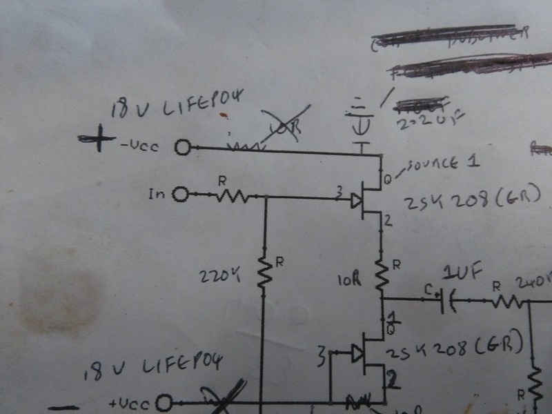
well the prototype has nearly no bypass caps, i was just leaving provision, previous experience with lifepo4 supplies suggests film bypass will be ok* swap Q2 and R3
* make the output track wider
* ground plane - try to keep the hi current ground (+/-33V) separate from signal ground. That applies to decoupling caps (C2/C3)
* try to add multiple pads for decoupling caps - to try various options. As far as I can see you play to use tantalum caps. Try to add pads for electrolytics on top.
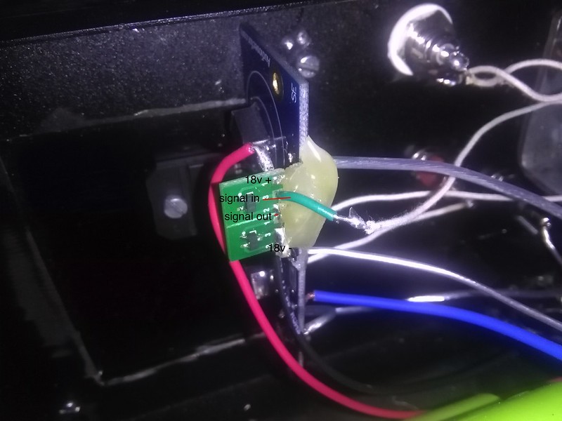
ill ask Enrico to look at the suggestions* jfet buffer power pins: try to arrange them in following order: +18, GND, GND, -18, also input GND should be close to power GND.


