Page 9 of 76
Re: It didn't explode....... YET (aka niges amp)
Posted: Thu Aug 18, 2016 11:12 pm
by nige2000
thanks guys
glad i posted pcb progress now
its as easy do it right as wrong
frd1996 wrote:Nige
Two cents from me:
* make +/-33V power tracks wider - much wider
* what is the value of R11,R12? What power do then need to dissipate?
yes brain definitely wasn't working there we will just bypass these resistors
* swap Q2 and R3
* make the output track wider
* ground plane - try to keep the hi current ground (+/-33V) separate from signal ground. That applies to decoupling caps (C2/C3)
* try to add multiple pads for decoupling caps - to try various options. As far as I can see you play to use tantalum caps. Try to add pads for electrolytics on top.
well the prototype has nearly no bypass caps, i was just leaving provision, previous experience with lifepo4 supplies suggests film bypass will be ok
* jfet buffer power pins: try to arrange them in following order: +18, GND, GND, -18, also input GND should be close to power GND.
ill ask Enrico to look at the suggestions
Re: It didn't explode....... YET (aka niges amp)
Posted: Fri Aug 19, 2016 5:43 pm
by frd1996
Hi Nige,
Since yesterday I've been thinking how I would draw your PCB. I decided to try and this is what came up. This is of course the first approximation of the final layout. I am not sure if I got the schematic and j-fet packages right. If you need the source files for this (DipTrace) then please give me a shout.
F
Re: It didn't explode....... YET (aka niges amp)
Posted: Sat Aug 20, 2016 12:30 pm
by nige2000
diptrace is actually what i was trying to learn
was the only one that made any sense to me
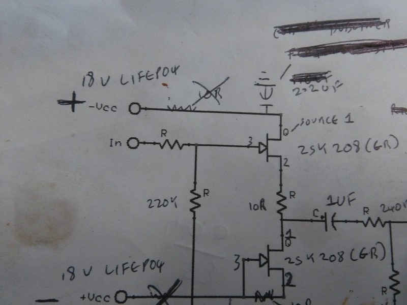
jfet buffer pin connections looks to be incorrect i know some jfets gave different pinouts ive used 2sk208 (gr) after sound testing a bunch of jfets
see prototype


think the 3875 circuit look ok

actually the more i think about resistors in series of lm3875 power input the more i fear it will slow the sheer speed of this amp we will likely end up shorting across
i like the routing of power and signal traces far less chance of cross contamination
maybe separate clean and dirty gnd connections to battery gnd/terminals might work better?
i see from this Peter seems to have put particular importance in a short feedback loop

maybe we can put a smd resistor between pin 3 and pin 8 on the underside
Re: It didn't explode....... YET (aka niges amp)
Posted: Sat Aug 20, 2016 1:01 pm
by jkeny
We must all be in sync - I recently started using Diptrace too - still in 30 day trial period - it seems the best eCAD package I could find too
Why do you need a pcb package when you have a hot glue gun? :)
If the +/- 33V supplies are from batteries then you don't need the R or C which are acting as a PS filter, I believe?
Separate ground returns for signal & PS are a good idea too
Short feedback loops were said to be the essence for the success of the sound of the Gaincard & the many DIY Gainclones that arose from it
Re: It didn't explode....... YET (aka niges amp)
Posted: Sat Aug 20, 2016 2:45 pm
by nige2000
jkeny wrote:We must all be in sync - I recently started using Diptrace too - still in 30 day trial period - it seems the best eCAD package I could find too
Why do you need a pcb package when you have a hot glue gun? :)
just tidier, more robust and easier to assemble and we need enough of them to be feasible
If the +/- 33V supplies are from batteries then you don't need the R or C which are acting as a PS filter, I believe?
pretty much agree i will likely bypass the r, the small film cap i doubt is doing any harm, i just put them in there to be more "PC" and leave the option
in fact i didn't use the r in series between dc decoupling cap and lm3875 signal input V+ on the prototype, nor any resistors in the jfet buffer which are supposed to prevent oscillations im told
Separate ground returns for signal & PS are a good idea too
yea think we should do that
Short feedback loops were said to be the essence for the success of the sound of the Gaincard & the many DIY Gainclones that arose from it
What you think should we try to put pads for an smd r between pin 3 and 8?
frd1996 if you're happy to finish off this pcb design Enrico will move on to something else?
still looking for better/easier cheaper relays to go between the ps's and cells
what you guys think of these
http://ie.farnell.com/te-connectivity-a ... dp/1326155
Re: It didn't explode....... YET (aka niges amp)
Posted: Sat Aug 20, 2016 3:33 pm
by jkeny
nige2000 wrote:jkeny wrote:We must all be in sync - I recently started using Diptrace too - still in 30 day trial period - it seems the best eCAD package I could find too
Why do you need a pcb package when you have a hot glue gun? :)
just tidier, more robust and easier to assemble and we need enough of them to be feasible
If the +/- 33V supplies are from batteries then you don't need the R or C which are acting as a PS filter, I believe?
pretty much agree i will likely bypass the r, the small film cap i doubt is doing any harm, i just put them in there to be more "PC" and leave the option
in fact i didn't use the r in series between dc decoupling cap and lm3875 signal input V+ on the prototype, nor any resistors in the jfet buffer which are supposed to prevent oscillations im told
Separate ground returns for signal & PS are a good idea too
yea think we should do that
Short feedback loops were said to be the essence for the success of the sound of the Gaincard & the many DIY Gainclones that arose from it
What you think should we try to put pads for an smd r between pin 3 and 7?
frd1996 if you're happy to finish off this pcb design Enrico will move on to something else?
still looking for better/easier cheaper relays to go between the ps's and cells
what you guys think of these
http://ie.farnell.com/te-connectivity-a ... dp/2251783
Yea, smd R would be a good idea
That's a latching relay - how are you unlatching it - reverse polarity?
This one is non-latching i.e turns off when power to coil is off
http://ie.farnell.com/te-connectivity-a ... dp/1326155
Re: It didn't explode....... YET (aka niges amp)
Posted: Sat Aug 20, 2016 4:45 pm
by nige2000
oops...... thats the one i meant to link
Re: It didn't explode....... YET (aka niges amp)
Posted: Sat Aug 20, 2016 10:19 pm
by frd1996
Hi,
I had some free time and worked on the amplifier board. It does not seem to be extremely difficult so I may finish it. I attach the schematic - please verify that this is correct. Few other informations:
* I verified the J-FET footprints - it matches the 2sk208 datasheet. Please double check it. The dot indicates the source pin.
* I removed R-C power filters. Instead I added footprints for small SMD caps - fully optional to install.
* _All_ capacitors and _all_ resistors are SMD 1206.
* The board got smaller 4x4 [cm].
* I will probably add vias between top and bottom GND copper pours.
Questions:
* What is the story with C1 (this is in the signal path). What type/size of capacitor do you anticipate there?
* Do you need any mounting holes, i.e. how the board will be mounted?
* Do you expect to use any connectors to connect the power/signal to the board, or all wires will be soldered?
Re: It didn't explode....... YET (aka niges amp)
Posted: Sat Aug 20, 2016 10:21 pm
by frd1996
The pictures of the board.
Re: It didn't explode....... YET (aka niges amp)
Posted: Sat Aug 20, 2016 11:00 pm
by nige2000
frd1996 wrote:Hi,
I had some free time and worked on the amplifier board. It does not seem to be extremely difficult so I may finish it. I attach the schematic - please verify that this is correct. Few other informations:
* I verified the J-FET footprints - it matches the 2sk208 datasheet. Please double check it. The dot indicates the source pin.
think its ok i must have misread it first time
* I removed R-C power filters. Instead I added footprints for small SMD caps - fully optional to install.
* _All_ capacitors and _all_ resistors are SMD 1206.
* The board got smaller 4x4 [cm].
* I will probably add vias between top and bottom GND copper pours.
Questions:
* What is the story with C1 (this is in the signal path). What type/size of capacitor do you anticipate there?
1210
* Do you need any mounting holes, i.e. how the board will be mounted?
would it not be ok to suspend it from the lm3875 chip
* Do you expect to use any connectors to connect the power/signal to the board, or all wires will be soldered?
probably just soldered
can you email me the diptrace files, maybe it will help me learn how to use it
