Page 11 of 21
Re: DIY Regen Battery tweak
Posted: Thu Jan 07, 2016 5:15 pm
by rickmcinnis
Well, the last thing I need are more of those isolator chips in my system!
At first I thought the thing was expensive but seeing the inside I guess it offers good value; there is so much stuff in there. YIKES!
Thanks for the pictures. Wasn't sure if this might have something to offer. Seems like a really complicated way to use the isolators.
What would the fpga do in a circuit like this, jkeny?
Does anyone recognize the USB hub? I wonder if this could be the one the REGEN guys say is "the best" but requires programming which is why they did not use it in the REGEN?
Re: DIY Regen Battery tweak
Posted: Thu Jan 07, 2016 5:35 pm
by randytsuch
jkeny wrote:Thanks for the pics, Pearse - very interesting
This device is regenerating the USB signal so it effectively does the same a the Regen but I see some potential weaknesses in that part of it's functionality
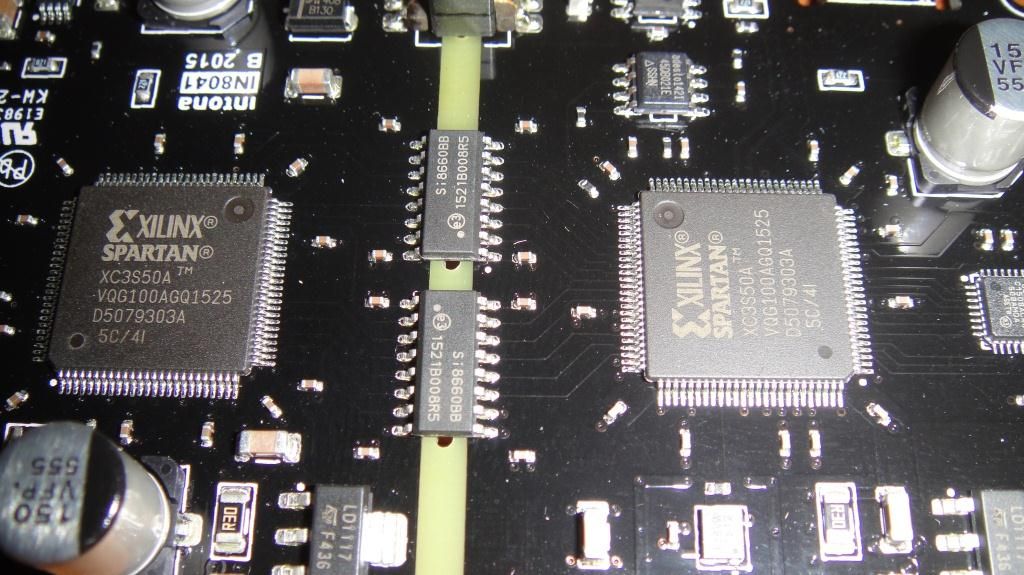
I can see that the device uses Xilinix FPGA to do the heavy lifting although the two chips (are they from FTDI?) between the FPGA & USB ports I would guess are responsible for translation to/from USB signal protocol. I see the isolators between the two sides of the board (giving 8 channels in each direction) & also the coilcraft transformer spanning the two sides of the board which I presume is responsible for the isolation of ground & +5V but I can't see how this can really provide clean PS on the other side - it is 5V on primary & 3.3V on secondary side - also the spec for the Intona says "Powered by USB host device; internal DC/DC converter for isolated side" - this whole PS area, I expect is a possible weak link although it appears to be helping SQ by isolating the other pathway for noise transference, the USB D+ & D- data lines
If the "clean" side was powered by a good PS supply, I reckon there would be some improvements. What I also don't see is a clock on the board but there is one black block that might be it ( I can't read the ID) - a decent clock with good PS might also be an improvement, I reckon.
But all very interesting - thanks for posting, Pearse
So for power, I'm guessing they are converting USB +5VDC to an AC voltage, passing the AC through the coilcraft transformer, and then rectifying the AC, and regulating it on the isolated side. You can't pass DC through a transformer, so I don't know another way to use USB 5V to power the isolated side.
I see three little linears on each side, probably to create 3.3V, and some lower voltages. Likely uses the lower voltage to power the FPGA, and another for the USB hub.
If you were brave enough, you could remove the coilcraft and supply 3.3V from a lifepo4, and also figure out if the other two regs will work from 3.3V, or if they need 5V (depends on their dropout voltage).
I would bet it would sound much better that way, versus how it is now, and maybe then you wouldn't need the regen.
Pierce,
Can you read the PN from the little square part between the FPGA (Xilinx part) and the connector?
The little square guy is the USB hub.
Randy
Re: DIY Regen Battery tweak
Posted: Thu Jan 07, 2016 6:23 pm
by jkeny
nige2000 wrote:is that two usb2412 chips on each end?
doubt theres any need for 5v on this
maybe new 3.3v supply?
Nearly but not quite - those chips are USB3320 USB transceivers from the same company SMC (Microchip) - so it's not regenerating the USB signal - the FPGA does this. These USB3320 chips need a reference clock from either an external clock or the clock signal comes in on a link from the FPGA chip - so unless the Xilinix has an internal clock, there has to be a clock on the board somewhere - the obvious candidate is what looks like an smd clock on the bottom right of Pearse's first set of pics

Re: DIY Regen Battery tweak
Posted: Thu Jan 07, 2016 6:36 pm
by jkeny
randytsuch wrote:
So for power, I'm guessing they are converting USB +5VDC to an AC voltage, passing the AC through the coilcraft transformer, and then rectifying the AC, and regulating it on the isolated side. You can't pass DC through a transformer, so I don't know another way to use USB 5V to power the isolated side.
Yea, that looks to be the case - DC to AC conversion ->transformer->AC to DC conversion.
I see three little linears on each side, probably to create 3.3V, and some lower voltages. Likely uses the lower voltage to power the FPGA, and another for the USB hub.
If you were brave enough, you could remove the coilcraft and supply 3.3V from a lifepo4, and also figure out if the other two regs will work from 3.3V, or if they need 5V (depends on their dropout voltage).
I would bet it would sound much better that way, versus how it is now, and maybe then you wouldn't need the regen.
But would still need a ground reference bridging the two domains - "dirty" & "clean".
If you left all the PS stuff in place, I wonder would connecting a 3.3V battery be an upgrade (the voltage coming from the trafo is 3.3V according to datasheet) ?
But other things probably also need to be addressed on the "clean" side - like the question of the clock & it's PS - this is usually the weakest link.
Pierce,
Can you read the PN from the little square part between the FPGA (Xilinx part) and the connector?
The little square guy is the USB hub.
Randy
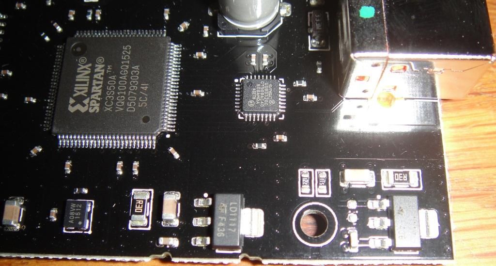
His next pics show it to be a USB transceiver
Re: DIY Regen Battery tweak
Posted: Thu Jan 07, 2016 6:52 pm
by jkeny
Sligolad wrote:Hi John,
I have the Intona before the Regen so just for the Isolation but as you say if it could do a good job of regenerating USB then maybe no need for Regen.
Does the Regen make a worthwhile difference to the sound with the Intona in line?
Below is probably the chip you are referring to and the other 2 pictures maybe help you are looking for clock, i could not see anything!!!
No, unfortunately no help for the clock chip identification
BTW, what was the landed cost of the Intona (you have the industrial version, I think?
Re: DIY Regen Battery tweak
Posted: Thu Jan 07, 2016 7:11 pm
by jkeny
Actually, I see it better in this later photo of yours

- the chip has 4 legs & id is A08VW 1512 - looks like a clock. The Xilinix FPGA can use a range of clock speeds from 5Mhz to > 320Mhz
So this clock? might be the timing foundation for the whole board.
Edit: Am I right that this clock? is on the USB input ("dirty") side of the board so a clock (from the FPGA) is distributed to the "clean" side of the board through the isolator chips - not the best solution, I reckon
Re: DIY Regen Battery tweak
Posted: Thu Jan 07, 2016 7:16 pm
by Sligolad
€362.95 John and this is the Industrial Version, I reckon the standard version would have been fine but.....
Re: DIY Regen Battery tweak
Posted: Thu Jan 07, 2016 7:53 pm
by sbgk
slightly off topic, question for JK
http://www.diyinhk.com/shop/audio-kits/ ... witch.html
Has received good review on head-fi, very detailed and analogue like.
Do you think the 48MHz oscillator is the key factor here ?
quote from specs -
"Newest XMOS chip and uses 48MHz oscillator to asynchronous reclock usb audio data to SPDIF line, old XMOS uses only 13Mhz oscillator, over 4x better jitter rejection theoretically."
Re: DIY Regen Battery tweak
Posted: Thu Jan 07, 2016 8:04 pm
by jkeny
sbgk wrote:slightly off topic, question for JK
http://www.diyinhk.com/shop/audio-kits/ ... witch.html
Has received good review on head-fi, very detailed and analogue like.
Do you think the 48MHz oscillator is the key factor here ?
quote from specs -
"Newest XMOS chip and uses 48MHz oscillator to asynchronous reclock usb audio data to SPDIF line, old XMOS uses only 13Mhz oscillator, over 4x better jitter rejection theoretically."
Difficult question - really don't know - could also be the internal workings of the new XMOS chip itself; could be the lower inductance of the BGA connector format; could be the driver; could be the external PS option - really impossible to tell.
Re: DIY Regen Battery tweak
Posted: Thu Jan 07, 2016 11:35 pm
by sbgk
jkeny wrote:sbgk wrote:slightly off topic, question for JK
http://www.diyinhk.com/shop/audio-kits/ ... witch.html
Has received good review on head-fi, very detailed and analogue like.
Do you think the 48MHz oscillator is the key factor here ?
quote from specs -
"Newest XMOS chip and uses 48MHz oscillator to asynchronous reclock usb audio data to SPDIF line, old XMOS uses only 13Mhz oscillator, over 4x better jitter rejection theoretically."
Difficult question - really don't know - could also be the internal workings of the new XMOS chip itself; could be the lower inductance of the BGA connector format; could be the driver; could be the external PS option - really impossible to tell.
I'm more tempted to try this than a regen, but interesting that each iteration of these devices seems to be moving in the right direction. Maybe wait a couple of years and it will all be perfect.

