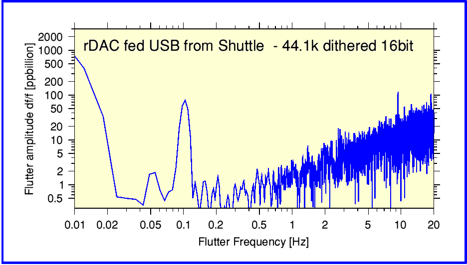
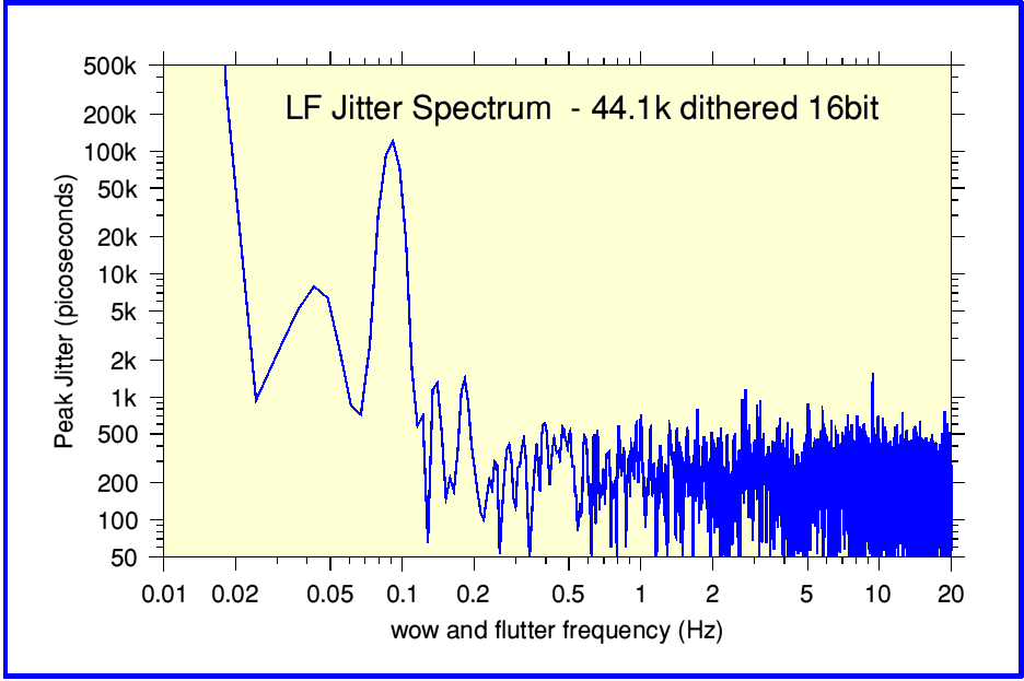
And here's JohnW's explanation of the plots
The process is called colour Grading - so from Black (no Waveform hits) to Red most Waveform "hit" areas.Originally Posted by adamdea View Post
John -thanks this is very interesting.
I'm not 100% sure what I'm looking at, could you help me to understand- is this in effect the plot of many many cycles of usb signal (voltage against time) overlaid ?
If the signal was perfect with no modulation then each waveform would overlay the previous and next waveforms and displayed as purely Red with no fluctuation from one cycle to the next (no other traces or colour) - the background would be Black.
"A digital phosphor oscilloscope (DPO) uses color information to convey information about a signal. It may, for example, display infrequent signal data in blue to make it stand out."
The scope timebase was 200pS a Div, so very fast any LF modulation causes the location of the eye pattern to shift in time - so the location of the crossing points fell into other areas which results these hits being colour graded - Lower Frequency events in Blue, more frequent events in light blue etc.Originally Posted by adamdea View Post
If it is then I can see that the main signal (high crossing to low and back again forming an x) is much sharper in the second case, showing much less fluctuation from one cycle to the next.
Also I see the difference in the background colour which I understand forms some sort of spuria. I also see that there are 3 green horizontal lines on the non-regen version - what are these (are they the rest state of the signal between data?)
The Green graded hits indicate "medium frequency events" - so these "odd states" happen frequently - Observing the Waveforms on a very fast Analogue scope "WITH IMAGE INTENSIFIER" to allow LF events to be visible on the CRT at such fast sweep speeds (500pS Div) you can see the "runt" events directly related to the processing tasks of the PC - the frequency of their occurrence is visibly modulated by the operating system workload / operation.
For sure any signal with unwanted modulation is not a good thing to have "flying around" a DAC PCB - these modulation effects will be very visible with an RF spectrum analyser looking at the Audio outputs - how the Audio system copes with this is anyone guess, and this is not the only mechanism this unwanted modulation can cross into the Analogue domain.Originally Posted by adamdea View Post
I'm trying to understand how we should interpret this information. I suppose it's difficult to be too prescriptive here because it's not clear what the transmission mechanism is for whatever undesirable results we are trying to eliminate
With any signal you need a return current path, as there is no such thing as true zero ohms ESPECIALLY at high frequency (Think GHz here with HS USB) the signal currents can be found almost everywhere on the PCB and internal to the silicon. So know you have unknown isolation attenuation between domains with such a signal, then its for sure a good thing to reduce any unwanted modulation of this signal.Originally Posted by adamdea View Post
1) the signal shape itself on the basis that it somehow directly affects the dac however it is read (as in your example of the jitter on the signal which somehow radiates within the dac even when the data is fed into a buffer via (in my words not yours) the glitch caused each time data is read into a buffer)
No, I totally don't agree with JS's hypothesis, I think John misses the main point about the unwanted modulation encoded within the USB signal - as the Colour graded plots clearly show.Originally Posted by adamdea View Post
2) the signal shape insofar as it causes the usb receiver to have to try hard to read the data (this is what I understand to be JS' hypothesis)
Yes, unrelated RF noise on the Data lines also needs to be attenuated which requires RF filtering - a separate function to the data repackaging / timing.Originally Posted by adamdea View Post
3 the noise in the signal (not the 5v line) which somehow pollutes the dac through some other mechanism
[have I got this right- are there other mechanisms I have missed]
Not directly related, but any noise on the 5V line (and this Ground) will couple into the Data lines, so should be avoided.Originally Posted by adamdea View Post
4) the noise on the 5v line (not not relevant to this plot I assume)
What do you think the Common Mode rejection performance will be at 1GHz? even my US$5K Tek test probe is only around 20dB CMR at 1 GHz, I can assure you that the USB Cable / interface will be less then this!Originally Posted by adamdea View Post
Having regard to those considerations (particularly the first and second). I'm trying to get my mind round the question of what it is about the signal that really matters. Am I right in thinking that because usb is a differential signal the receiver would automatically ignore the common mode noise, as it would be reading the difference signal?
Yes, I seem to have awoken some deep seated concerns - but atleast I have been ale to measure quite a significant modulation of the USB Data related to the CPU / System processing which opens the possibility that the "Bodge fix" attempts of optimised software players might have a foundation in "reality" - although they are a very wrong / incomplete band aid to a problem that should not be allowed to cross into or even effect the analogue domain.Originally Posted by adamdea View Post
Apologies for the rambling, I'm just trying to work out what this all means.

